
Making high-brightness red Micro-LED chips for augmented reality and virtual reality devices has been fraught with various difficulties. Now Kubos Semiconductors has come up with a little-known material and thinks it could solve this problem. As the major tech giants scramble to launch various AR and VR devices to provide users with the vivid and bright images they have been waiting for, they have finally encountered such a common bottleneck: the development of red Micro-LED chips. The luminous efficiency of all current LEDs plummets as the device size decreases due to inherent material defects that have a severe impact at very small device sizes. Among them, the red LED is particularly obvious.
According to reports, UK-based startup Kubos Semiconductors recently came up with a solution that they believe could solve the problem. "The development of red Micro-LED chips has been keeping people awake at night because no one can make the traditional gallium nitride materials used in the manufacture of blue and green LED devices work effectively in the longer red wavelength band." Chief executive Caroline O'Brien said: "If you want to find a breakthrough, you have to look at the problem in a different way. And that's what we've been doing."
So, what are the problems encountered in the development of red Micro-LED chips? The practical problem is that shrinking a typical blue LED from its current commonly used size to a size of 5 microns drops its luminous efficiency from around 90 percent to around 40 percent. Although there has been a large drop, it is already acceptable from an application point of view. In the same situation, for red LEDs, the luminous efficiency will drop from 60% to about 1%. Such a large drop is the crux of the current problem, and the main reason for this difference lies in the materials used to manufacture these devices. different.
To date, blue and green LEDs have typically been made from indium gallium nitride (InGaN) material. However, when developers also use InGaN materials to manufacture longer-wavelength red LED devices, the subtle differences in material composition can generate strong polarization fields in the light-emitting region of the device, and it is this polarization field that greatly reduces luminous efficiency. Therefore, most device manufacturers began to choose to use indium gallium phosphide (InGaP) semiconductor material to manufacture red LED devices. This approach has worked well until Micro-LED applications and their scaling issues.
In fact, startups around the world are currently concentrating on the manufacture of red Micro-LEDs. South Korean UV LED manufacturer Soft Epi is improving the luminous efficiency of GaN-based red Micro-LEDs by adjusting the growth process. Micledi, a spin-off company of Imec in Belgium, recently announced the successful launch of an AlInGaP Micro-LED chip that emits "Ferrari red" color light. In the UK, Cambridge University spin-off startup Porotech has developed porous GaN wafers, which they call PoroGaN, and believe this will be the basis for making Micro-LED chips that can emit light of various colors. In addition, Porotech has recently teamed up with Wales-based compound semiconductor wafer supplier IQE to develop wafer products.
Amid this increasingly active technology development activity, though, Kubos Semiconductor still insists that a common material system is the ultimate way forward for blue, green and red Micro-LEDs. For the startup's executives, the material that could win the future is another GaN. While much of the industry's love for GaN has focused on alloys with a hexagonal crystal structure, Kubos Semiconductors founder David Wallis, also of Cardiff and Cambridge universities, has been working on a cubic GaN for years. Due to the higher crystal symmetry of cubic GaN, this GaN variant is immune to the strong polarization fields that, as mentioned above, reduce the luminous efficiency of GaN-based red LEDs.
So why is everyone paying attention to GaN, which has a hexagonal crystal structure? In fact, as early as the 1990s, research on the growth of cubic GaN began to stagnate, because this material may be thermodynamically unstable, which makes it very difficult to grow this material with high quality on most substrates. Around the same time, research into the growth of hexagonal GaN took off, and as the pace of device development picked up, most researchers slowly began to forget about cubic GaN.
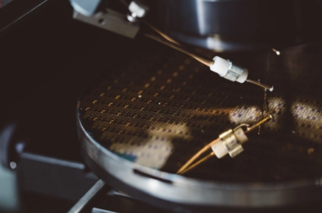
Still, Wallis and his colleagues insisted on growing cubic GaN on a wafer with a thin SiC substrate. Anvil Semiconductor, a subsidiary of the University of Warwick in the UK, was the first to design silicon-based SiC substrates for developers of SiC power electronics. Later, Wallis and his team successfully developed a stable process for growing cubic GaN on the above-mentioned substrate, and established Kubos Semiconductor Company based on this achievement. Since then, the company has been producing 150mm wafers, growing cubic GaN using the industry-standard metal-organic chemical vapor deposition (MOCVD) process.
"Silicon substrates are compatible with CMOS processes, and because of the low lattice mismatch between thin SiC layers and cubic GaN, we can force the growth of GaN into the cubic state," O'Brien said. The cost of this SiC thin layer will be significantly reduced, which also allows our full set of solutions to start competing with the current Micro-LED manufacturing methods that use quantum dots or grow GaN on sapphire substrates."
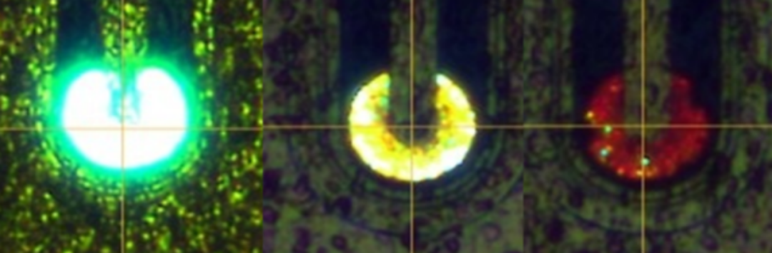
Kubos intends to grow cubic GaN on larger 200mm SiC wafers on silicon, which according to O'Brien is "the real sweet spot." Kubos CEO Caroline O'Brien believes that the numerous patents accumulated around its cubic GaN process have given the company a great commercial advantage. In addition, she also pointed out that only a few players in the industry are currently researching cubic gallium nitride, such as the University of Illinois at Urbana-Champaign and Rensselaer Polytechnic Institute in the United States and the University of Paderborn in Germany. Moreover, these research institutions are currently Neither have yet developed commercial devices. Kubos recently fabricated a 50-micron diameter cubic GaN unpackaged Micro-LED chip that emits red light. From this, they hope to prove that it is possible to manufacture longer wavelength Micro-LEDs using the cubic GaN scheme. Currently, the company is increasing its wafer supply to allow customers to customize its proprietary red Micro-LED chips. According to O'Brien's estimates, the external quantum efficiency of these initial LED devices is about 3%.
This technology and light-emitting devices will undoubtedly be very good news for technology giants that are working hard to produce high-resolution, high-brightness AR/VR smart glasses, and it will also allow Kubos Semiconductors to gain more and more benefits in the future. Many companies have favored and even acquired invitations.
Post time: Mar-27-2023