In the field of high-definition RGB display chips, front-mount, flip-chip and vertical structures are "three pillars", among which ordinary sapphire front-mount and flip-chip structures are more common, and vertical structures usually refer to thin-film LED chips that have been stripped from the substrate. A new substrate may be fixed or the substrate may not be bonded to make a vertical chip.
Corresponding to display screens with different pitches, the advantages and disadvantages of front-mount, flip-chip and vertical structures are different, but no matter comparing the front-mount structure or the flip-chip structure, the advantages of the vertical structure in some aspects are obvious.
P1.25-P0.6: Four advantages stand out
Lattice has compared the performance of Lattice’s vertical 5×5mil chips and JD formal 5×6mil chips through experiments. The results prove that compared with the front-mounted chips, the vertical chips have no side light due to single-sided light. There is less light interference as the spacing becomes smaller. In other words, the smaller the pitch, the less brightness loss. Therefore, vertical chips have obvious advantages in luminous intensity and display clarity at smaller pitches.
Specifically, the vertical chip has a bright light emitting shape, uniform light output, easy light distribution, and good heat dissipation performance, so the display effect is clear; in addition, the vertical electrode structure, the current distribution is more uniform, and the IV curve is consistent. The electrodes are on the same side, there is current blockage, and the uniformity of the light spot is poor. In terms of production yield, the vertical structure can save two wires compared with the ordinary formal structure, and the wiring area in the device is more sufficient, which can effectively increase the production capacity of the equipment and reduce the defect rate of the device due to wire bonding by an order of magnitude.
In display applications, the "caterpillar" phenomenon has always been a major problem for manufacturers, and the root cause of this phenomenon is metal migration. Metal migration is closely related to the temperature, humidity, potential difference and electrode material of the chip, and it is more likely to appear in a display with a smaller pitch. The full vertical chip structure also has natural advantages in solving metal migration.
First, the distance between the positive and negative poles of the vertical structure chip is greater than 135 μm. Due to the large distance between the positive and negative poles in the physical space, even if metal ion migration occurs, the lamp bead life of the vertical chip can be more than 4 times longer than that of the horizontal chip, which greatly improves product reliability and stability. It's better for flexible display. The second is that the surface of the blue-green chip with a vertical structure is an all-inert metal electrode Ti/Pt/Au, which is difficult for metal migration to occur, and its main performance is the same as that of a red-light vertical chip. The third is that the vertical structure chip uses silver glue, which has good thermal conductivity, and the temperature inside the lamp is much lower than that of the formal installation, which can greatly reduce the migration speed of metal ions.
At this stage, in the P1.25-P0.9 application, although the ordinary front-mounted solution occupies the main market due to its low price advantage, the flip-chip and vertical solutions play a major role in high-end applications due to their higher performance. In terms of cost, the price of a group of RGB chips in the vertical solution is 1/2 that of the flip-chip solution, so the cost performance of the vertical structure is higher.
In P0.6-P0.9mm applications, ordinary front-mount solutions are limited by the physical space limit, it is difficult to guarantee yield, and the possibility of mass production is low, while flip-chip and vertical chip solutions can meet the requirements. It is worth noting that, for the packaging factory, it is necessary to add a large amount of equipment to adopt the flip-chip structure scheme, and because the two pads of the flip-chip are extremely small, the yield rate of solder paste welding is not high, and the maturity of the packaging process of the vertical chip scheme High, the existing packaging
factory equipment can be used in common, and the cost of a set of RGB for vertical chips is only half of that of a set of RGB for flip-chips, and the overall cost performance of the vertical solution is also higher than that of the flip-chip solution.
P0.6-P0.3: Blessing of two major technical routes
For P0.6-P0.3 applications, Lattice mainly focuses on Thin Film LED, a thin film chip technology without substrate, covering vertical structure and flip chip structure. Thin film LED generally refers to a thin film LED chip that has been stripped from the substrate. After the substrate is stripped, a new substrate can be bonded or a vertical structure can be made without bonding the substrate. It is called Vertical thin film, or VTF for short. At the same time, it can also be made into a flip-chip structure without bonding the substrate, which is called thin film flip chip, or TFFC for short.
Technical route 1: VTF/TFFC chip + quantum dot red light (QD + blue light InGaN LED)
Under the extremely small chip size, the traditional AlGaInP red LED has poor mechanical properties after the substrate is removed, and it is extremely easy to break during the transfer process, making it difficult to carry out subsequent mass production. Therefore, one solution is to use printing, spraying, printing and other technologies to place quantum dots on the surface of GaN blue LEDs to obtain red LEDs.
Technical Route 2: InGaN LEDs are used in all RGB colors
Due to the insufficient mechanical strength of the existing quaternary red light after removing the substrate, it is difficult to carry out subsequent process production. Another solution is that the three colors of RGB are all InGaN LEDs, and at the same time realize the unification of epitaxy and chip manufacturing. According to reports, Jingneng has started the research and development of gallium nitride red light on silicon substrates, and some achievements have been made in silicon-based InGaN red light LEDs, making it possible for this technology.
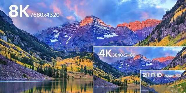
It is worth noting that, by comparing the advantages and disadvantages of TFFC, FC, and Micro chips in terms of substrate, chip separation, luminous efficiency, and mass transfer, Lattice came to a conclusion: using Micro’s technical route and Lattice’s The combination of Mini chips can greatly reduce chip costs while reducing technical difficulty. This also means that 4K and 8K Mini ultra-high-definition LED large-screen products are expected to enter thousands of households.
At present, 4K and 8K Mini ultra-high-definition display large screens are unstoppable driven by 5G technology, and silicon substrate vertical Mini LED chips have the opportunity to become a super cost-effective light source solution.
Post time: Nov-18-2022