
In recent years, domestic chips have faced the danger of "stuck neck". Some experts have discussed that China can either build domestic chips along the technical route of foreign countries, or find another way and open up a new track to achieve overtaking in corners. Obviously, the latter route is more difficult. At present, these two routes are parallel, and each has a breakthrough.
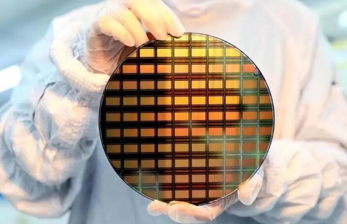
Domestic photoelectric chip manufacturing achieves nanoscale for the first time
On the evening of September 14, Chinese scientists published their latest research in the world's top academic journal "Nature". For the first time, they obtained a nanoscale light-engraved three-dimensional structure, making a major breakthrough in the field of next-generation photoelectric chip manufacturing. It is better for flexible led screen. This major invention may open up a new track for photoelectric chip manufacturing in the future, and is expected to be used in the fabrication of key photoelectric device chips such as photoelectric modulators, acoustic filters, and non-volatile ferroelectric memories. It has broad application prospects in 5G/6G communication, optical computing, artificial intelligence and other fields.
photoelectric industry pearl, widely used downstream
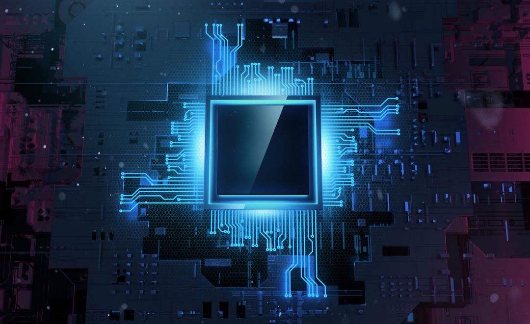
Optical chips are the core components in the field of photoelectric. photoelectric devices (referred to as optical chips in China) are an important subdivision of the global semiconductor industry. With the vigorous development of the photoelectric semiconductor industry, optical chips, as the core components of the upstream industry chain, have been widely used in communications, industry, consumption, etc. many fields. According to Gartner's classification, photoelectric devices include CCD, CIS, LED, photon detectors, photoelectric, laser chips and other categories.
As the core components of the photoelectric industry, optical chips can be divided into active optical chips and passive optical chips according to whether photoelectric signal conversion occurs. Active optical chips can be further subdivided into transmitting chips and receiving chips; passive optical chips It mainly includes optical switch chips, optical beam splitter chips, etc. It is also used in P1.56 flexible screen. In this report, we focus on the industrial development trend, market space and localization opportunities of active optical chips such as laser chips and photon detection chips.
There are many sub-categories of optical chips, and the industry covers a wide range of fields. In addition to the active/passive classification above, optical chips can also be divided into four categories: InP, GaAs, silicon-based and thin-film lithium niobate according to different material systems and manufacturing processes. The InP substrate mainly includes direct modulation DFB/Electro-absorption modulation EML chips, detector PIN/APD chips, amplifier chips, modulator chips, etc. GaAs substrates include high-power laser chips, VCSEL chips, etc. Silicon substrates include PLC, AWG, modulator, optical switch chips etc., LiNbO3 includes modulator chips, etc.
Optical chips usher in development opportunities
For half a century, microelectronics technology has developed rapidly in accordance with Moore's Law. It's better for led display industry. The problem of power consumption has increasingly become a bottleneck that is difficult for microelectronics technology to solve. The development of electronic chips is approaching the limit of Moore's Law, and it is difficult to continue to seek breakthroughs in the electronic computing technology paradigm. In the potentially disruptive technology facing the "post-Moore era", optical chips have entered people's field of vision. Optical chips are generally made of compound semiconductor materials (InP and GaAs, etc.), and realize the mutual conversion of photoelectric signals through the generation and absorption of photons accompanied by the internal energy level transition process.
Optical interconnection can also improve the communication capacity within the transmission medium by using a variety of multiplexing methods (such as wavelength division multiplexing WDM, mode division interoperability MDM, etc.). Therefore, the on-chip optical interconnection based on the integrated optical circuit is considered to be a very potential technology, which can effectively break through the bottleneck of the physical limit of traditional integrated circuits. The localization of optical modules, fiber lasers, lidars and other mid- and downstream links in the industrial chain is progressing smoothly. At present, my country's downstream
segments such as optical modules, fiber lasers, and lidars have strong competitiveness, and the localization of related fields will continue to advance. In terms of optical modules, according to statistics released by Lightcounting in May 2022, Chinese manufacturers will occupy six of the top ten optical module manufacturers in the world in 2021.
The progress and way out of China's optical chip industry
In the domestic market, driven by the substantial expansion of downstream demand in recent years, domestic manufacturers have tried to build China's optical chip industry through technology research and development, foreign acquisitions and other methods. The lack of domestic high-end optical chips has brought huge development opportunities to the industry. With the support of policies, my country's optical chip industry has developed rapidly. It's good for transparent led screen. Especially in recent years, the international situation has been unstable, and incidents of foreign supply of domestic chips have occurred frequently. Domestic substitution has also become a hot topic in the domestic semiconductor industry in recent years, relying on the continuous efforts of some leading domestic optical chip companies.
For China, it is necessary to make up for shortcomings in the field of traditional electronic chips as soon as possible, but also to make efforts in the layout of new circuits such as photoelectric chips as soon as possible. With two-pronged approach, efforts will be made to seize the opportunity of a new round of technological revolution and industrial transformation.
Post time: Dec-02-2022